Embedded systems RAM and flash consumption examples
Client RAM and flash consumption are impacted by:
- The board itself - board target code and network driver sizes vary.
- Bootloader sizes for the board vary from 26 KiB to 58 KiB. A custom bootloader with required functionality under 10 KiB is possible, but a standard free offering is larger.
- Network stacks vary in size from tens of kilobytes (AT parser-based solutions) to megabytes (some Wi-Fi and cellular stacks).
- Compiler - GCC_ARM, Arm Compiler and IAR all behave differently and produce binaries with different sizes.
- Compiler settings - optimizations for speed or size have an impact on the generated code.
- C/C++ language features and libraries used in an application - Client does not use the C++ Standard Library (STL), as it adds 15 KiB of ROM consumption.
- Feature selections:
- Adding a filesystem, for example for SD card or external flash, adds tens of kilobytes of code and kilobytes of RAM.
- Enabling traces can almost double flash consumption.
- Additional drivers or application logic:
- Bluetooth stack takes 80-150 KiB.
- A complex sensor driver can take several tens of kilobytes of flash.
Example configurations
- IAR version 8.32.1 (V8.32.1.169/LNX) compiler.
- Release profile used when compiling with
-DMBED_HEAP_STATSflag. - Memory figures in the table include all memory usage (Mbed OS, Client example application, Mbed TLS, networking stack).
- Firmware update capability is included.
| Item | Client min config | Client max config | Client Lite |
|---|---|---|---|
| Board | NXP K64F | NXP K66F | NXP K64F |
| Connectivity | ESP8266 *1 |
Ethernet (lwIP) | ESP8266 *1 |
| Client version | 4.0.0 | 4.0.0 | 0.9.0 |
| Mbed OS version | 5.14.0 | 5.14.0 | 5.13.0 |
| Storage | KVstore (TDBStore (internal)) | KVstore (TDBStore (internal)) | NVStore |
| Features | All optional disabled | All enabled | All enabled *2 |
| Config file | esp8266_minimal.json |
eth_v4.json |
ram-minification.json |
The minimal configuration drops all non-essential Client features, such as:
- First-to-claim.
- Device-generated certificates.
- Blink patterns from the example application.
Example memory figures
Memory consumption figures measured using the Client (or Client Lite) example application:
| RAM consumption | Client min config | Client max config | Client Lite |
|---|---|---|---|
| RAM, static (KiB) | 22 | 54 | 27 |
| RAM, dynamic (KiB) | 30 | 46 | 18 |
| RAM, total (static + dynamic, KiB) | ~52 | ~100 | ~45 |
RAM peak dynamic consumption is mostly driven by the TLS handshake.
| ROM consumption (flash, KiB) | Client min config | Client max config | Client Lite |
|---|---|---|---|
| Bootloader size | 32 | 32 | 32 |
| KVStore allocation (NVStore for Lite) | 48 | 96 | 8 |
| Application and Mbed OS size | 273 | 369 | 185 |
| Firmware update download area | 273 | 369 | 185 |
| Total (flash, KiB) | 626 | 866 | 410 |
Note: The allocations in internal flash must always be aligned to the flash erase sector size. So, even if the bootloader size is only 29 KiB, the erase sector size may force you to allocate 32 KiB for it. Erase sector sizes are chipset-specific, so check your chipset specification. This also applies to the firmware download area.
We provide multiple bootloaders. Configurations using SPI flash or SD card as firmware download storage are approximately 10 KiB larger as they have to include block device and SD driver. We can also provide a custom optimized bootloader that fit into 10 kilobytes. Contact Arm Professional Services for the optimizations.
*1 ESP8266 Wi-Fi has flow control (CTS, RTS) and reset connected with updated firmware (v1.7).
*2 The Client Lite feature set differs greatly from the Client feature set, and is therefore not comparable to Client.
Example flash memory layout - internal flash only
Typically, the most optimal solution is an internal-flash-only layout. You can optimize the bootloader and OS, as there is no need for SPI/QSPI drivers.
A high-level example of an internal-flash-only layout:
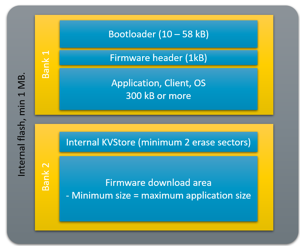
Note: Dual-bank flash is mandatory.
Due to the nature of flash memory, the erase cycle prevents simultaneous reads from the same bank. This has a notable impact on application execution. Network stacks with high latency requirements can quickly get out of sync during an erase operation if internal KVStore is located in the same bank as the application. Memory map data and code regions must also be aligned to flash banks because executing code from a bank being written or erased leads to undefined behavior. Please refer to the hardware reference manual of the chipset you are using.
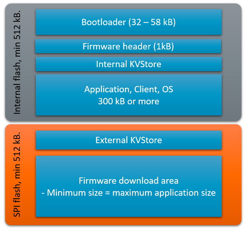
Example flash memory layout - internal flash and SPI flash
If the application is large or you need to store large amounts of application data, this solution can be the most cost-effective. However, this increases the size of the bootloader and OS, as you need storage drivers, and possibly a filesystem. The firmware download area can be located in the SPI flash, which decreases the size of the internal flash significantly. (Q)SPI flash memories are also usually rated to 100 000 erase cycles so flash wearing is not an issue.
A high-level example of internal flash and SPI flash layout: